Home
News
New Products
Exhibitions
RHEED
Systems
Accessories
Software
RHEEDVision
RHEEDVision Pro
RHEEDVision Pro DigiTen
RHEED Gun Control
kSA 400
TorrRHEED™
RHEED Imaging Analyzer
Products
PEEM
PEEM Control
PEEM Vision
IEEM
Ion Sources
Electron Guns
Fine Focus
General Purpose
Low Energy
Flood Guns
High Power
Analyzers
RHEA-100
SuperCMA Family
Single Pass - ESA
Double Pass - DESA
WinSpectro XP
PEEM
UHV SEM
WinSpectro SEM
WinSpectro SAMSEM
SEM Accessories
EBSD
Company
Contact
PEEM
PEEM Control
PEEM Vision
IEEM
Ion Sources
Electron Guns
Fine Focus
General Purpose
Low Energy
Flood Guns
High Power
Analyzers
RHEA-100
SuperCMA Family
Single Pass - ESA
Double Pass - DESA
WinSpectro XP
PEEM
UHV SEM
WinSpectro SEM
WinSpectro SAMSEM
SEM Accessories
EBSD
PEEM
P
hoto
E
mission
E
lectron
M
icroscopy
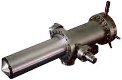
PEEM System
oval and chemical
defects on GaAs
integrated
circuit
YBaCuO
superconductor
passivated
InP
layer deposited
by ablation
chemical image
of InP
crystal phases
on YBaCuO
growth defect
on YBaCuO
test
pattern
large defect
on GaAs
stressed
GaAs
integrated
circuit