NANOFOCUS SEM package
THE new STAIB NANOFOCUS is a Schottky field emitter type based scanning electron microscope. The compact and affordable system is ideally suited as an add-on to existing UHV surface analysis chambers, or as a basis for a highly versatile UHV SEM-SAM (Scanning AUGER Microscopy) system.
The NANOFOCUS SEM package consists of:
- the electron gun with full octopole stigmator / deflection stage and double alignment
- the high voltage supply
- the scanning and beam control supply
- the USB gun control and scanning interface
- the USB image acquisition interface
- one Windows XP PC with 19" TFT display
- the control and image acquisition software
- and the low noise scintillator type secondary electron detector (optional)
 |
||||||||
 |
||||||||
 |
||||||||
Integrated control and imaging software
The full WINDOWS software allows for the complete control of all gun parameters and furthermore of the optional STAIB secondary electron detector. All parameter sets can be saved and retrieved through simple windows operations.
The gun control and the image acquisition use USB interfaces. No cumbersome additional internal PCI cards are needed.
The image acquisition performs with up to 12 frames per second. These live images can be integrated during operation with selectable integration time by simple application of a linear slide, leading to very low noise SEM images.
A unique software controlled gun parameter wobbling simplifies the gun adjustment.
The operator can choose between several preset configurations for energies and/or beam current just by selecting a windows button.
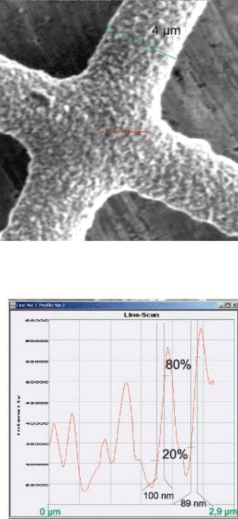
The acquired images can be saved and exported. The images can be calibrated for magnification, and distances can be measured through a line scan.
In case of external x and y inputs for Scanning AUGER Microscopy, the image acquisition is halted, but all gun control parameters can still be controlled.
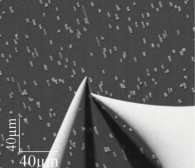
Resolution test (for 32 mm working distance)
Resolution test (for 20 mm working distance)
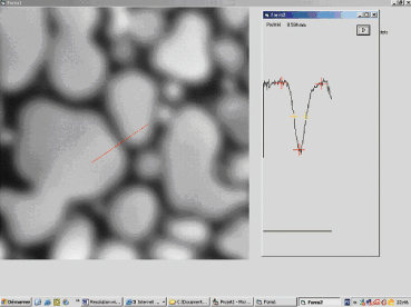
Silver islands on a Carbon substrate. FWHM 47 nm +/- 4 nm.
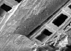
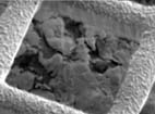
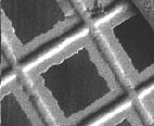
Example for STM wiring of Ag islands on silicon