| PEEM
Photo Emission Electron Microscopy |
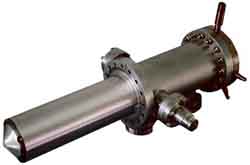 PEEM System |
 oval and chemical defects on GaAs |
 integrated circuit |
 YBaCuO superconductor |
 passivated InP |
 layer deposited by abblation |
 chemical image of InP |
 crystal phases on YBaCuO |
 growth defect on YBaCuO |
 test pattern |
 large defect on GaAs |
 stressed GaAs |
integrated circuit |
![]()
![]()
![]()